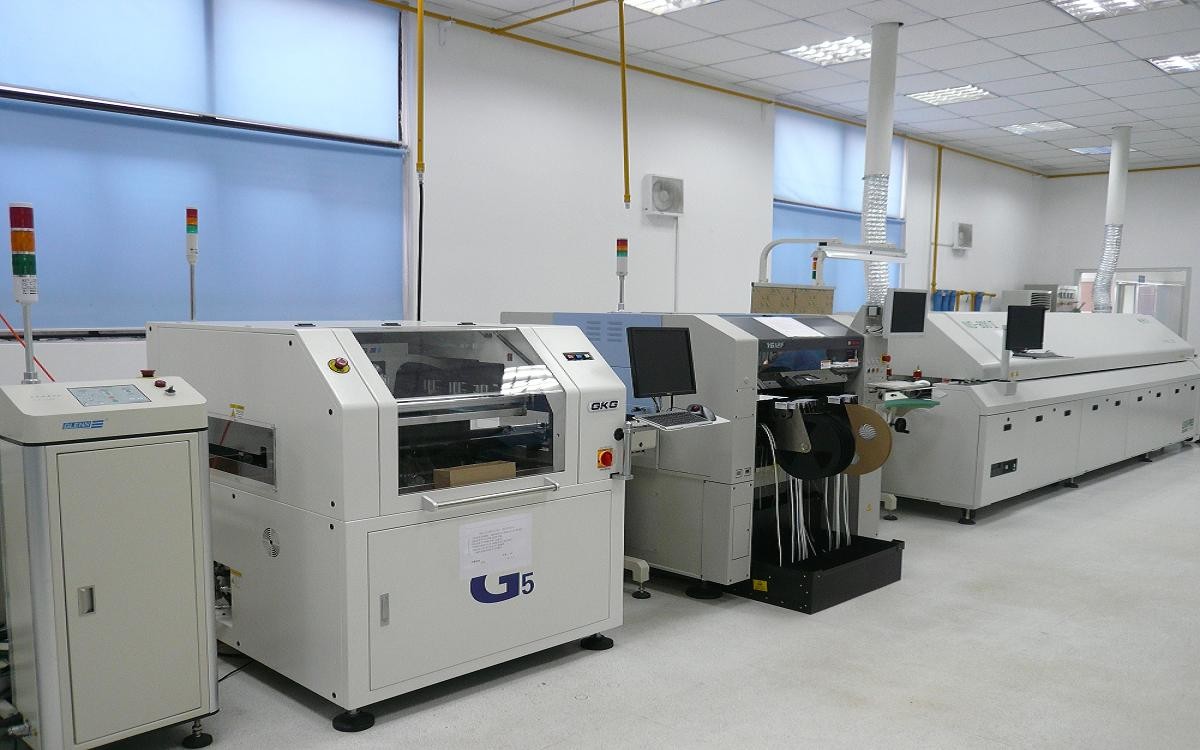
Once the surface mount components are soldered in place after the reflow process, which doesn't stand for completion of PCBA and the assembled board needs to be tested for functionality. Often, movement during the reflow process will result in poor connection quality or a complete lack of a connection. Shorts are also a common side effect of this movement, as misplaced components can sometimes connect portions of the circuit that should not connect.

Checking for these errors and misalignments can involve one of several different inspection methods. The most common inspection methods include:
• Manual Checks: Despite upcoming development trend of automated and smart manufacturing, manual checks are still relied on in PCB assembly process. For smaller batches, an in-person visual inspection by a designer is an effective method to ensure the quality of a PCB after the reflow process. However, this method becomes increasingly impractical and inaccurate as the number of inspected boards increases. Looking at such small components for more than an hour can lead to optical fatigue, resulting in less accurate inspections.
• Automatic Optical Inspection: Automatic optical inspection is a more appropriate inspection method for larger batches of PCBAs. An automatic optical inspection machine, also known as an AOI machine, uses a series of high-powered cameras to "see" PCBs. These cameras are arranged at different angles to view solder connections. Different quality solder connections reflect light in different ways, allowing the AOI to recognize a lower-quality solder. The AOI does this at a very high speed, allowing it to process a high quantity of PCBs in a relatively short time.

• X-ray Inspection: Yet another method of inspection involves x-rays. This is a less common inspection method — it's used most often for more complex or layered PCBs. The X-ray allows a viewer to see through layers and visualize lower layers to identify any potentially hidden problems.
The fate of a malfunctioning board depends on PCBA company's standards, they will be sent back to be cleared and reworked, or scrapped.
Whether an inspection finds one of these mistakes or not, the next step of the process is to test the part to make sure it does what it's supposed to do. This involves testing the PCB connections for quality. Boards requiring programming or calibration require even more steps to test proper functionality.
Such inspections can occur regularly after the reflow process to identify any potential problems. These regular checks can ensure that errors are found and fixed as soon as possible, which helps both the manufacturer and the designer save time, labor and materials.


 你的文字必须在20- 3000个字符之间!
 请检查您的邮箱号是否正确
  你的文字必须在20- 3000个字符之间!
 请检查您的邮箱号是否正确

